Third, solder mask printing materials
Solder resist is also one of the most commonly used materials for printed boards. It coats the surface of the printed board with a layer of permanent protective film to selectively shield the wire patterns from damage, and will not be brazed. A short circuit occurs, and the film-forming substance has good chemical resistance, solvent resistance, heat resistance, and good insulation properties. It has the functions of moisture-proof, mildew-proof, and salt-spray resistance, and it also has an aesthetic effect on printed boards.
The main color of the solder mask is green, but also red, yellow, blue, transparent and other colors. The surface condition of the film can be divided into several patterns, plain, matt and bright. The classification of solder resist printing materials can also be divided into three categories: thermosetting, light-curing, and liquid-sensitive. No matter what type of solder mask, the film-forming material must have the following good properties (see Table 1). .
Table 1 Properties of film forming substances
Characteristics Hardness Pencil hardness 6H Adhesion 100% (3M tape test) Thermal shock resistance 260°C 10 s × 5 times Insulation Normal temperature ≥ 1013 Ω; After hot flash ≥ 1012 Ω Solvent resistance and acid-base solution Good flame resistance US UL standard 94V - Level 0 (1) Thermosetting
The thermosetting solder mask is mainly composed of epoxy resin or modified epoxy resin, curing agent, fillers, auxiliaries, pigments and solvents. Through the action of the curing agent, cross-linking reaction occurs to form a three-dimensional network structure, which is divided into one liquid type and two liquid type.
a. The curing agent has been added to the one-component type printing material, which is very convenient to use. Because there is no need to add curing agent, there is no artificial factor such as inaccurate weighing and uneven mixing between the two. The printing material will not be cured on the screen, but the effective use time of the printing material is short, which is only 1 to 2 months and the storage conditions are relatively high.
b. The two-liquid type is divided into the main agent and the auxiliary agent. Before use, the mixture should be weighed according to the ratio. Mix and stir evenly and stand still for 30 minutes to eliminate bubbles and fully mature. The use of a mixture of most branded printing materials is 24 h (hours). The best use period is 1/4 to 1/2 of its service life. During this time, the closer it is to its useful life, the lower its printability will be, and the lower the leveling property will be, the easier it will be to stop the net, and the use of unfinished printing materials will be discarded and thrown away, but due to the main agent and Separate additives, it is a longer storage time, up to 6 months.
The physical properties of thermosetting solder masks, such as pencil hardness, adhesion, and toughness, are related to drying temperature, drying time, and film thickness. The higher the curing temperature, the longer the time and the more the coating becomes. Thick, cross-link bridging can be a good, high molecular weight coating.
Drying and curing conditions are: hot air circulation oven, temperature 140-150°C, time 30-40 min, and it is more common to use double-layered and multi-layered boards with epoxy glass cloth as a base material.
(2) Photosetting
Ultraviolet (UV) curable printing materials consist of unsaturated resins with double bonds, photosensitive monomers, sensitizers, fillers and additives. Under the irradiation of ultraviolet light (200-400 nm), the free radicals of the printed material generate a chain polymerization reaction, and this reaction is rapid and completes in an instant (in seconds), forming an insoluble and infusible high molecular polymer. The operating process conditions are as follows: 80 W/cm 3 high-pressure mercury lamps, irradiation distance 10 cm, and conveying speed 4-6 m/min.
The UV-curable printing material has many advantages. Due to the absence of solvents, the solid content is 100%, the viscosity will not change during screen printing, the film layer will not be thinned, shrinkage deformation will occur, and there will be no pollution to the environment. Screen printing It does not block the screen plate, absorbs UV light and has a fast curing speed and high production efficiency. It is suitable for automated production of high-volume assembly lines.
Single-sided printed board production mostly uses light-curing types. In addition to the above reasons, because single-sided printed boards use paper substrates more, they require shorter baking times and lower temperatures. If the temperature is high and the time is long, the board warps and deforms. At the same time, the thickness of the copper foil on the single-sided printed board is 35 μm, and the film layer of the printed material is thin, and the ultraviolet light easily penetrates the film.
The double-sided or multi-layer printed boards are mostly thermoset type. Due to thick copper and secondary copper plating, the thickness of the copper foil is 50 to 70 μm. The ultraviolet light penetrating ability is limited, and sometimes the bottom part is printed The material cannot be cured or not completely cured, causing wrinkling or partial peeling of the solder resist layer during hot-air leveling or wave soldering (Figure 1).
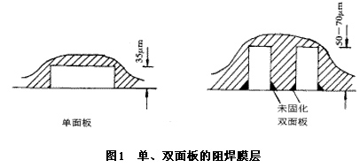
Figure 1 Single and double-sided solder mask layers
When the solder mask layer of the fine printed board adopts the traditional screen printing process, skipping may occur due to fine lines and narrow spacing. When the scraper squeegees from right to left, there is a step at the back of the scraper A, the amount of ink is less, the coverage is incomplete, the edge of the copper foil will be exposed, at the corner of the wire will also have a thin solder mask Phenomenon, easy to produce poor insulation between the leads; at the same time in the B facing the scraper, due to ink bleeding, in the connecting plate will be stained with ink, in the hot air leveling can not touch the solder, or in the welding of welding, etc. Bad welding phenomenon (Figure 2).
Figure 2 Screen printing of the solder mask layer of a fine printed board
Huayao Master (Puyang) Automation Equipment Co., Ltd. , https://www.huayaolive.com